
👋 Guest author Ashley Lin studies science, technology, and international affairs at Georgetown University.
If you follow the tech headlines, you might have heard about one Taiwanese company’s critical role in fabricating leading-edge computer chips, or one Dutch company’s monopoly in the machinery needed. But even though semiconductors are now front and center in tech policy discussions, many other potential chip chokepoints are far from the headlines—and even when you know what inputs to look for, it can be difficult to assess their role in the chip production process and the geopolitical context surrounding them.
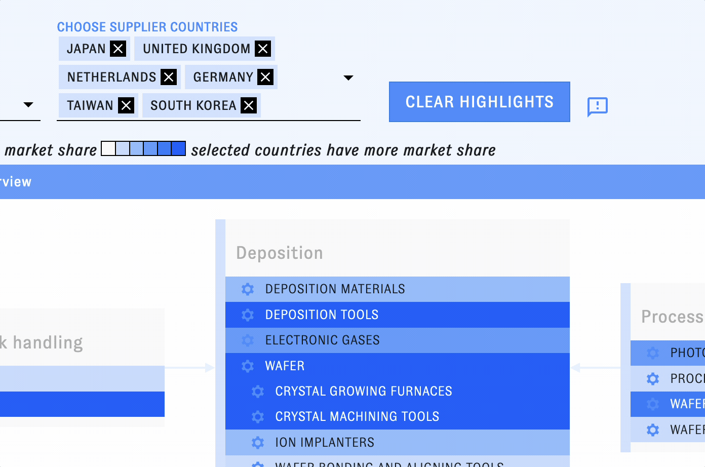
Fortunately, our Supply Chain Explorer can help you get up to speed. The Explorer draws out potential chokepoints with a “Market Concentration” highlighter, which shows chip inputs supplied by a few countries. Inputs highlighted in dark blue have higher market concentration. For example, when you apply the “Market Concentration” highlighter, dark blue highlights jump out in the “Wafer and photomask handling” and “Deposition” fabrication steps.

You can also use the “Supplier Countries” filter to the same effect for specific countries. For example, selecting the U.S. and some of its key allies and partners - we entered Japan, the Netherlands, the UK, Germany, Taiwan, and South Korea - shows how dominant these countries are across many stages of the supply chain. Most supply chain segments are highlighted in dark blue, except for wafer bonding and aligning tools (the U.S. and Germany nonetheless supply 18% of the market share) and integrated assembly tools (Singapore holds 98% of the market share).
However, it's worth going one step further. Clicking on each input in the Explorer reveals details about the input’s role in the chip fabrication process, its relative value and complexity, its global market share, and the number of supplier countries. These details reveal that some chokepoints matter strategically more than others. While all are worth knowing, the Explorer can help unearth lesser-known chokepoints and illustrate how they shape semiconductor geopolitics.
1. The U.S. leads in design, but design may be difficult to monopolize
Less publicized chokepoints: core chip intellectual property (52% U.S./43% UK), electronic design automation software (96% U.S.)
According to the Explorer, the U.S. captures 52% of the global market share in core intellectual property (IP) and 96% in the electronic design automation (EDA) software used to design chips. UK-based, Japanese-owned ARM holds another 43% of the global core IP market share, meaning that the U.S. and its allies have 95% of the core IP market total.
However, the US' strong position in core IP and EDA software has not kept other countries from the design game. Browse the Explorer, and you'll see that many other nations–including China, Taiwan, South Korea, and various European countries–capture meaningful shares of the broader design market for logic chips. What’s more, inputs to chip design, such as software and intellectual property, are easier to transfer and use compared to physical equipment in the chip supply chain, making logic chip design potentially more difficult to control over the long term.
2. Chokepoints in wafer production and bonding are geographically distributed and less strategic
Less publicized chokepoints: wafer bonding and aligning tools (83% Austria’s EV Group)
The first step in fabrication–turning designs into chips–is wafer production. This involves cutting semiconducting material into disk-shaped wafers, which are later processed and packaged into individual chips. Production of crystal growing furnaces and crystal machining tools are highly concentrated—but the Explorer explains that this equipment has “relatively low value and complexity,” which suggests it may be easier for countries to spin up domestic production or alternatives. Similarly, though Japan has an 88% market share for wafer handlers, the technology is described as “relatively less complex.” The Explorer shows that in addition to Japan, the U.S., South Korea, Taiwan, France, and China all produce this input, which may indicate they could scale up production if needed.
Wafer bonding and aligning tools used to join silicon wafers are primarily produced by Austria’s EV Group (83%) and Germany’s SUSS MicroTec (13%). Although chokepoints in the wafer production process are often viewed as less strategically important than lithography, deposition, and etch tools–for example, it was not prominent in early U.S. chip export controls–the Explorer highlights how “the wafer production process” encompasses multiple steps. Certain inputs, like wafer bonders, could be worth a second look from policymakers given their geographic concentration.
Get updates
3. Deposition heavily relies on the U.S.
Less publicized chokepoints: Rapid thermal processing tools (90% U.S.’ Applied Materials), ion implanters (U.S. is the primary supplier)
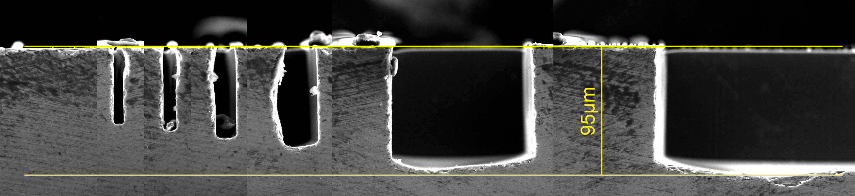
After wafer production, several fabrication processes create patterns and devices in each wafer: adding new layers of different materials to the wafer (“deposition”), drawing circuit patterns in the layer (“photolithography”), carving the pattern into the permanent wafer layer, and removing the etched material (“etch and clean”). We often hear about where major fabrication facilities (“fabs”) are located, but regardless of location, fabs rely on equipment produced worldwide.
For example, consider the “deposition” step, where specialized tools deposit and modify thin films of material on a silicon wafer. Many types of deposition tools are dominated by a single country, such as high-temperature CVD tools (75% U.S.’ Applied Materials), plasma CVD tools (91% U.S.’ Applied Materials and Lam Research), electrochemical coating tools (100% U.S.’ Applied Materials and Lam Research), physical vapor deposition tools (92% U.S.’ Applied Materials and KLA), rapid thermal processing tools (90% U.S.’ Applied Materials, Mattson Tech, and Veeco), and tube-based diffusion and deposition tools (84% Japan’s Kokusai and Tokyo Electron).
The Explorer notes that rapid thermal processing tools are a particularly significant chokepoint among these deposition tools because they are critical to several steps in chip fabrication. While they rarely make the headlines, rapid thermal processing equipment and other deposition tools have been an initial focus and key target of U.S. export controls since the degree of U.S. leadership in market share creates a chokepoint for other countries.
4. Advanced photolithography relies on Japan—not just the Netherlands
Less publicized chokepoints: Advanced photomasks (53% Japan/40% U.S.), maskless lithography equipment (dominated by Japan’s JEOL/NuFlare and Sweden’s Mycronic), resist processing tools (96% Japan’s Screen and Tokyo Electron)
The Netherlands enjoys a dominant position in advanced photolithography equipment. Extreme ultraviolet (EUV) scanners are necessary for mass-producing the most advanced logic chips and are exclusively built by the Dutch firm ASML. As reported in WIRED, “The current generation of EUV machines are already, to put it bluntly, kind of bonkers. Each one is roughly the size of a bus and costs $150 million… Only a few companies can afford the machines, and most of them go to the world’s big three leading-edge chipmakers: the world’s leading foundry, Taiwan-based TSMC, as well as Samsung, in South Korea, and Intel.”
ASML is in the news a lot now, but there's much more to advanced photolithography than EUV. A step down from EUV scanners is deep ultraviolet (DUV) scanners, specifically ArF immersion, the only lithography tools capable of mass-producing near-cutting-edge chips. It is important to not rule out DUV. For example, DUV equipment is widely reported to have enabled China’s SMIC to develop seven-nanometer chips, used in Huawei’s 5G phones. Both immersion and dry ArF scanners are also produced by the Japanese firm Nikon (Japan has a 43% market share of dry ArF scanners and 9% of ArF immersion scanners; ASML produces the rest), giving Japan an important role in older lithography tools. Both the Netherlands and Japan have imposed export controls on EUV and some DUV (ArF immersion) scanners.
Other chokepoints in photolithography are even less publicized. Advanced photomasks, required to transfer circuit patterns onto chips, are primarily supplied by three countries: Japan (53%), the United States (40%), and Taiwan (7%). Resist processing tools (“tracks”) needed to coat photoresists on wafers for EUV and DUV photolithography are solely produced by Japan’s Screen and Tokyo Electron (96%). Other countries, such as Germany, China, and South Korea, produce less advanced tracks. Finally, maskless lithography equipment production is dominated by single countries; for example, Japan’s JEOL and NuFlare produce 91% of electron-beam tools, and Sweden’s Mycronic produces 97% of laser lithography tools. Maskless lithography variants are slow at drawing patterns into wafers and thus unsuitable for mass chip production. However, they are cost-effective for producing low-volume items, such as prototypes or chips for specific use cases that don’t require scale.
5. Japan and the U.S. lead etch and clean
Less publicized chokepoints: Dry etching and cleaning tools (dominated by the US and Japan), wet etching and cleaning tools (72% Japan’s Screen and Tokyo Electron)
Etching and cleaning tools are necessary to "set" the patterns produced by photolithography and remove surrounding material. In particular, "dry" etching and cleaning tools, which are faster and can create finer details, are needed for the most advanced chips. The U.S. and Japan dominate the main types of dry etching tools: conductor (84% US’ Applied Materials and Lam Research, 16% Japan’s Hitachi and Tokyo Electron) and dielectric (60% Japan’s Tokyo Electron, 36% US’ Lam Research). The Explorer notes that though China’s AMEC also produces dry-etching tools for TSMC’s 7 and 5 nm nodes, they are not used for the finest features, such as complex transistor structures. Like deposition and lithography, etching and cleaning tools have been a focus of recent U.S. export controls.
Meanwhile, wet etching and cleaning tools are also dominated by Japan’s Screen and Tokyo Electron (72% market share) and the US’ Lam Research (16% market share). Wet etching is not typically used for the smallest features, though it can be cheaper, risks less damage to substrates, and etches more precisely on smaller areas.
To access the Supply Chain Explorer, visit chipexplorer.eto.tech or check out the full documentation for more context. As always, feel free to get in touch if you need additional support – we are always glad to help. 🤖